
Knowledge Mining: The Future of Automated Analog Layout Synthesis
Analog layout synthesis with knowledge mining
This paper introduces a novel knowledge-based analog layout synthesis methodology that automates the generation of new circuit layouts by mining and reusing design expertise from legacy, quality-approved layouts. By employing graph-based pattern matching and a maximum-weight-clique formulation, it achieves high layout reusage rates, significantly reducing manual design effort.
TL;DR
Analog layout design remains the "black art" of the semiconductor world—highly manual and dependent on tribal knowledge. This paper presents a methodology that treats legacy layouts as a knowledge database, breaking them down into reusable patterns. By matching new schematics against this database and solving for the maximum reusage rate, the system can synthesize high-quality layouts that preserve human-expert preferences in milliseconds.
Problem & Motivation: Why Analog Automation is Hard
In the digital world, RTL-to-GDSII is a well-oiled machine. In analog, we still rely on experts. Why?
- Implicit Constraints: Design rules (like symmetry or common-centroid) are just the tip of the iceberg. Experts have "feelings" about parasitics and signal integrity that are hard to quantify.
- Topology Rigidity: Existing migration tools (like those using symbolic templates) require the new circuit to be nearly identical to the old one. If you change a single transistor configuration, the template breaks.
The authors' insight is: Don't try to migrate the whole layout; migrate the patterns. Even if a new circuit is unique, it is often composed of building blocks (differential pairs, current mirrors, OTAs) that have been laid out successfully before.
Methodology: The "Lego" Approach to Circuit Design
The methodology consists of three sophisticated stages:
1. The Design Knowledge Database
The system converts legacy schematics into Connection Graphs. To handle the complexity of transistor terminals (Drain, Gate, Source, Bulk), they introduced a Universal Coding Scheme. This allows the graph to uniquely identify how devices are interconnected through a mathematical sum (), capturing the logical topology and physical constraints simultaneously.
2. Pattern Matching and Selection
This is the "brain" of the operation. Given a target schematic, the tool searches the database for the largest possible common sub-circuits.
- The Problem: Many potential patterns might overlap. You can't use two different legacy layouts for the same transistor.
- The Solution: They construct a Pattern Graph where nodes represent possible pattern matches and edges represent "compatibility" (no shared devices). By finding the Maximum-Weight-Clique, the tool selects the optimal combination of patterns to maximize the "Reusage Rate."
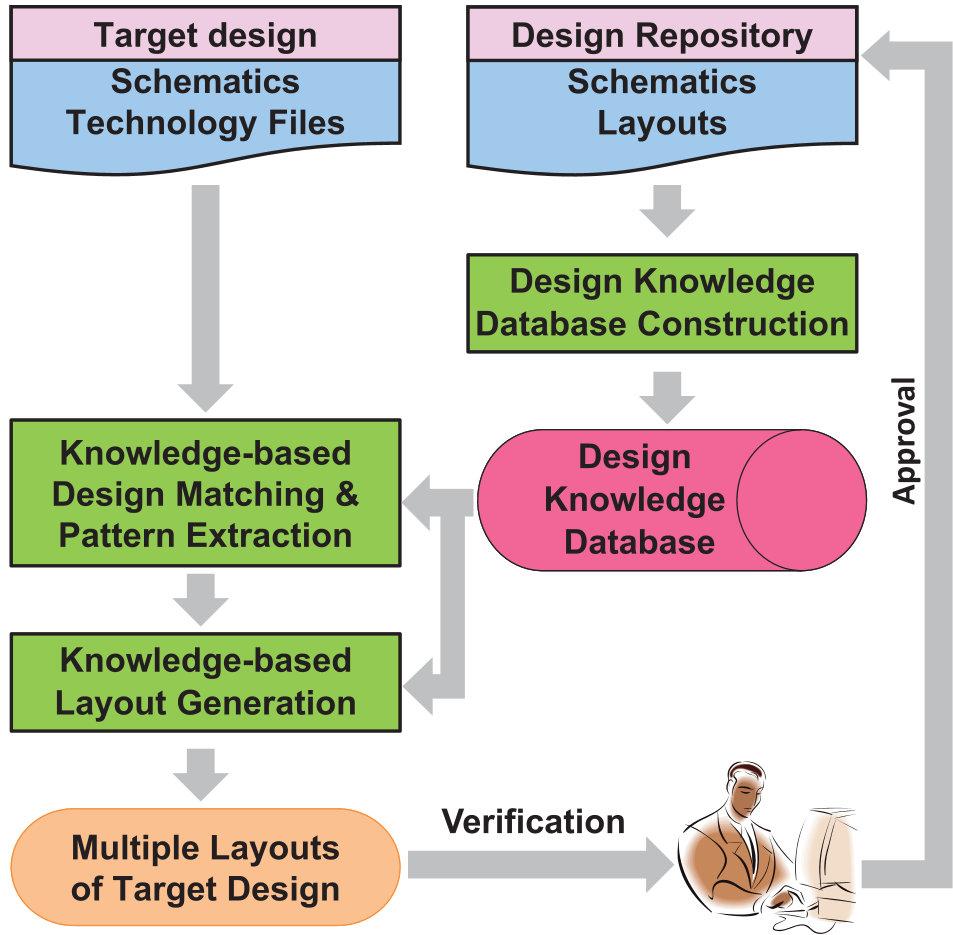 Fig 1: The proposed knowledge-based synthesis flow, from database construction to final generation.
3. Layout Assembly
Once patterns are chosen, the tool extracts the corresponding physical polygons, migrates them to the target technology, and uses Hierarchical B-trees* to pack these rectilinear blocks together. Remaining "unconnected" nets are then handled by an inter-pattern router.
Experimental Validation
The authors tested this on a Class-AB Operational Amplifier (38 devices, 78 nets). They started with an empty repository and gradually added legacy designs:
- With 1 Legacy (Diff Amp): 66% device reuse.
- With 3 Legacies (Diff Amp, OTA, Miller Op-Amp): 100% device reuse and 60% net reuse.
 Table 1: The correlation between the size of the "Knowledge Base" and the resulting layout reusage rate.
As seen in the visual comparison (Fig 5 in the paper), the final synthesized layout (d) looks remarkably professional because it literally "copy-pastes" the placement and routing strategies optimized by humans in the source layouts (a, b, and c).
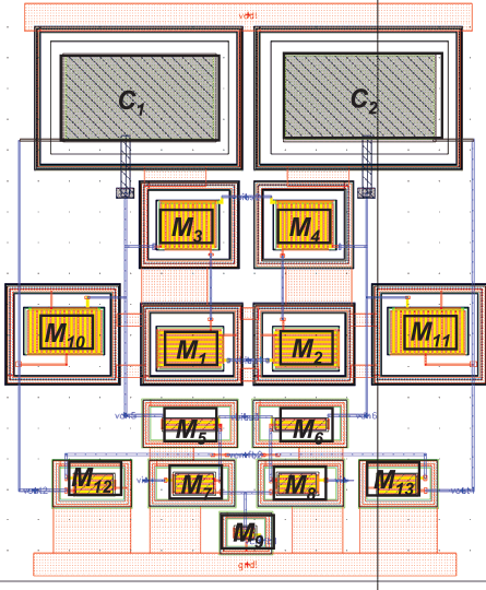 Fig 2: Visual evidence of design expertise preservation. The synthesized Class-AB Op-Amp (d) inherits the structured blocks of its ancestors.
Critical Insight & Conclusion
This work shifts the paradigm of Analog EDA from "Optimization from Scratch" to "Intelligent Component Reuse."
Takeaway: The key to automating analog design isn't just better physics solvers; it's better data management. By building a repository of "Golden Layouts," companies can ensure that new designs inherit the reliability of the old ones.
Limitations: The current approach assumes that legacy layouts are available and "quality-approved." Furthermore, the inter-pattern routing (the 40% of nets not reused) still relies on traditional routing algorithms, which may not always match the expert quality of the internal pattern routing.
Future Work: Integrating this graph-matching approach with modern Machine Learning (like Graph Neural Networks) could allow the tool to "generalize" patterns even when they aren't exact matches, further pushing the boundaries of automation.