
To DFT or Not to DFT: A Deep Dive into the Economics of Testability
TO DFT OR NOT TO DFT? The answer depends on who is asking and who is answering. Designers might view DFT as a necessary evil that prevents them from achieving the best possible design-"best" meaning high performance, minimum hardware complexity, and low power. From the test engineer's perspective, "best" may be quite different-controllability, observability, and diagnosability being the desired attributes. From a manager's or marketing perspective, "best" includes both sets of attributes-but in the form of costs incurred versus benefits gained. Likewise, for us "best" means an end product that maximizes the cost-to-benefit ratio, with the decision to use DFT ultimately based on its impact on profit. 1 Decision-makers typically make test tradeoffs using models that mainly represent direct costs such as test generation time and tester use. Analyzing a test strategy's impact on other significant factors such as test quality and yield learning requires an understanding of the dynamic nature of the interdomain dependencies of test, manufacturing, and design. Our research centers on modeling the tradeoffs
The paper introduces the Carnegie Mellon University (CMU) Test Cost Model, a comprehensive framework for modeling the economic tradeoffs of Design-for-Testability (DFT). It quantifies the cost-benefit ratio across design, manufacturing, and test domains, identifying critical thresholds where DFT becomes profitable.
Executive Summary
TL;DR: The decision to implement Design-for-Testability (DFT) is often a tug-of-war between designers seeking performance and test engineers seeking observability. This paper presents the CMU Test Cost Model, which transcends simple hardware overhead calculations by modeling the "Total Cost of Quality," including hidden factors like test escapes and yield learning. The study reveals that while DFT increases silicon area, its ability to accelerate manufacturing maturity and reduce the shipment of defective parts makes it economically superior for most large-scale or high-reliability applications.
Academic Context: This work serves as a foundational bridge between VLSI design and economic manufacturing theory, moving the DFT debate from qualitative intuition to quantitative simulation.
The "Evil" vs. The "Necessary": Defining the Problem
Traditionally, DFT is viewed as a "necessary evil." Designers hate it because it consumes area and can degrade performance. However, evaluating DFT based solely on is a mistake. The authors argue that the true "best" design is one that maximizes the cost-to-benefit ratio.
Previous models were too siloed. They ignored the fact that a more testable chip isn't just easier to test—it's easier to fix in the factory. The motivation here is to link the test floor back to the bottom line by modeling interdomain dependencies.
Methodology: The Anatomy of the CMU Test Cost Model
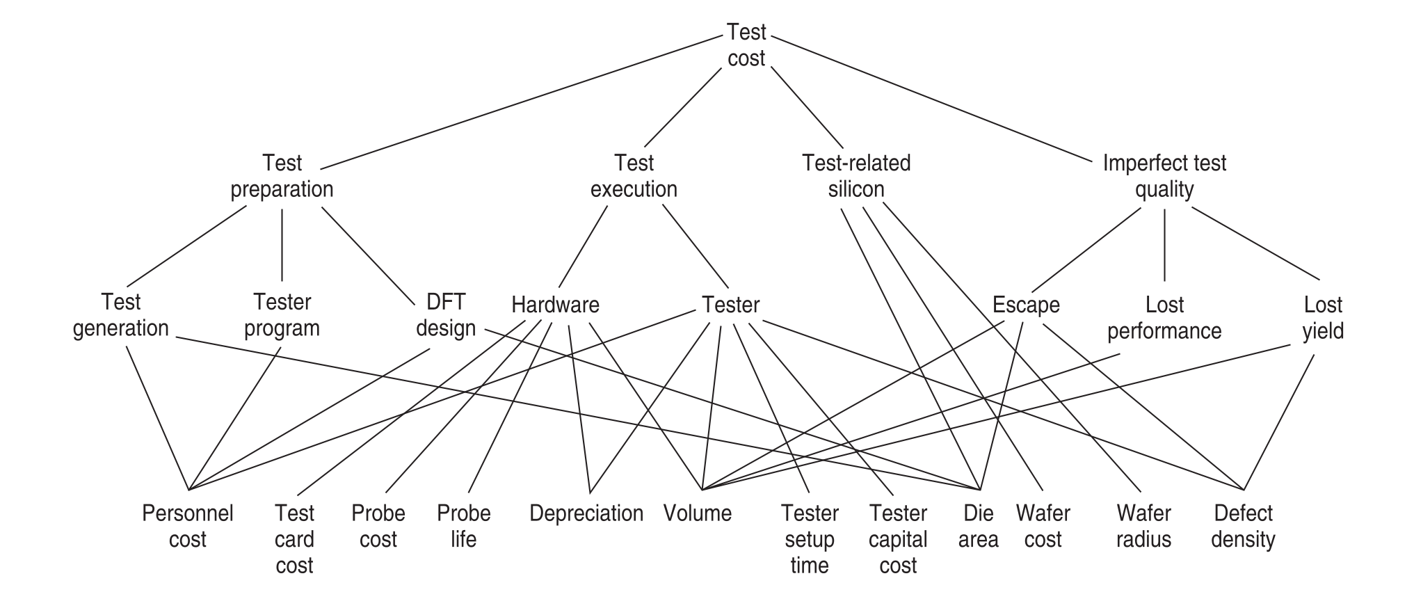
The model defines the total test cost per good die () through four primary pillars:
- Preparation Cost (): NRE costs like ATG and test program creation.
- Execution Cost (): The actual time spent on the ATE (Automated Test Equipment).
- Silicon Cost (): The physical area overhead and its impact on yield.
- Imperfect Quality Cost (): The "hidden" cost of shipping bad chips (escapes).
The Dependency Tree
The complexity of the model is captured in its hierarchical structure, where physical parameters (like die area) drive higher-level economic outcomes.
The Alpha Factors: Modeling the Shift
To compare DFT vs. non-DFT, the authors introduce Alpha Factors (). These are modifiers that represent the improvement (or penalty) DFT brings:
- : The area overhead (typically 5-13%).
- : The reduction in time for generating test patterns (often 90% reduction).
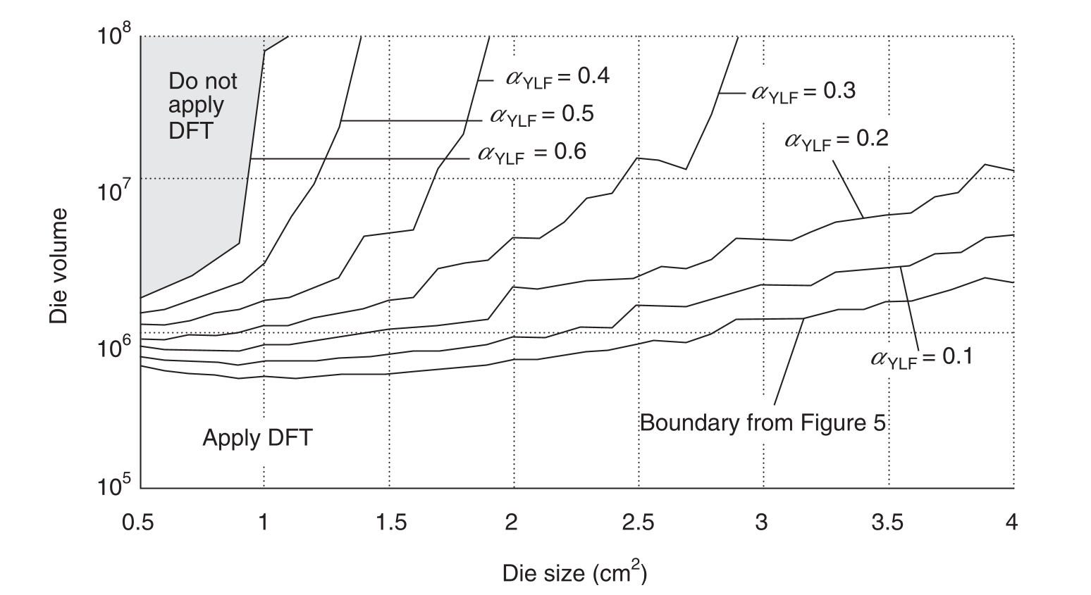
- (Yield Learning Factor): This reflects how much faster the manufacturing defect density () drops because DFT allows for better diagnosis.
Experimental Analysis: Finding the Breaking Point
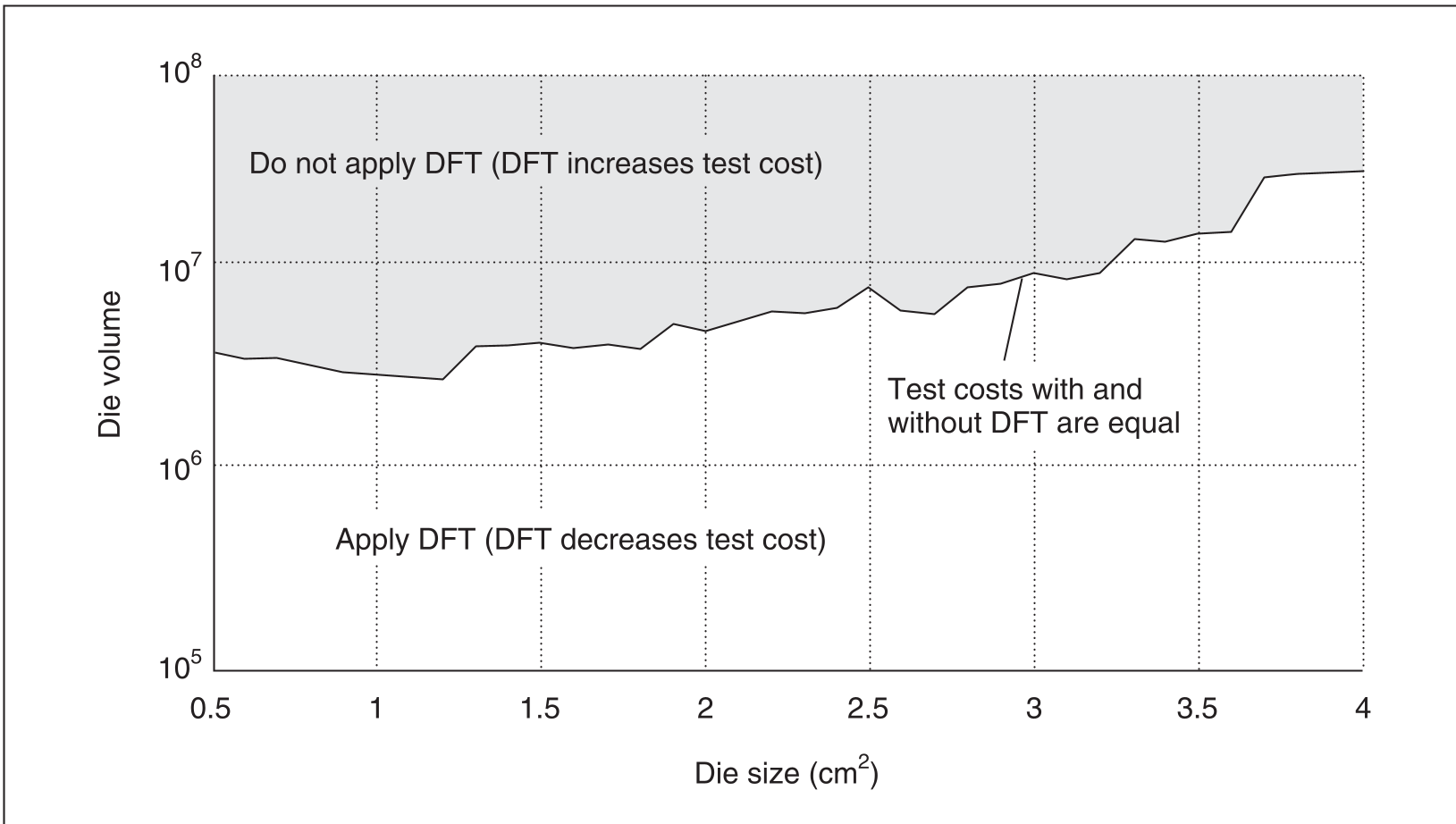
The authors simulated various scenarios by varying production volume () and die area ().
The "Profitability Domain"
In a "Best Case" scenario (low overhead, high efficiency), DFT dominates almost the entire die-size/volume plane. However, as overhead increases, an Uncertainty Region emerges.
The Game Changers: Escape Costs and Yield Learning
The most striking finding is the impact of Test Escape. If the risk of shipping a bad chip is high (), the "Apply DFT" region expands dramatically to cover high-volume microprocessors. Similarly, for large dies, the yield is inherently lower, making the diagnostic benefits of DFT (Yield Learning) the deciding factor for profitability.
Critical Insights & Future Outlook
- Area is King: The model shows that has the most significant impact on the worst-case boundary. Minimizing overhead is the most effective way to justify DFT.
- Volume vs. Quality: While high-volume ASICs might seem to favor no-DFT due to silicon costs, the "economic penalty" of a single field failure can flip the decision instantly.
- Limitations: The model assumes a fixed technology node. In modern FinFET processes, the relationship between area and yield is even more non-linear, suggesting that the model needs updates for nanometer-scale effects.
Final Takeaway: DFT is an insurance policy. The "premium" is the silicon area, but the "payout" is a faster ramp to market and a protected brand reputation. As architectures move toward System-on-Chip (SoC), partitioning these models for different cores (Memory BIST vs. Logic Scan) will be essential for modern EDA workflows.