
HOY Methodology: Is Wireless Communication the Antidote to Skyrocketing IC Test Costs?
Economic Analysis of the HOY Wireless Test Methodology
This paper introduces the HOY (Hypothesis, Odyssey, and Yield) wireless test methodology, which replaces traditional wired Automated Test Equipment (ATE) with a wireless communication interface and on-chip Design-for-Test (DFT) circuits. The study proposes a comprehensive test cost model to quantify the economic advantages of wireless testing for System-on-Chip (SoC) devices.
Executive Summary
TL;DR: The semiconductor industry has long struggled with a paradox: while chip manufacturing costs drop with each node, test costs remain stubbornly high. The HOY (Hypothesis, Odyssey, and Yield) methodology proposes a radical shift—eliminating the physical "umbilical cord" (wired probes) of traditional Automated Test Equipment (ATE) in favor of a wireless, BIST-heavy architecture. This transition reduces test costs by up to 74%, primarily by slashing the massive capital expenditure required for high-end testers.
Positioning: This work serves as a foundational economic and architectural framework for non-contact testing, moving it from a theoretical "academic curiosity" to a viable industrial roadmap for SoC and 3D IC production.
The Problem: The Inflexible Cost of Wired Testing
In the deep-submicron era, chips are becoming faster and denser, but the equipment used to test them has stalled in terms of cost-efficiency. Traditional testing relies on:
- Expensive Probes: Probe cards for ultra-fine pitches are costly and prone to wearing out (limited "touch-downs").
- High Pin Counts: Increasing complexity forces chips to have more PADs, taking up valuable silicon real estate just for testing.
- ATE Depreciation: High-end testers cost millions, and as test times increase, the cost per die scales linearly with the time spent on the machine.
Methodology: The HOY Wireless Infrastructure
The HOY approach reimagines the DUT (Device Under Test) as a self-contained unit capable of receiving commands and reporting results via RF signals.
1. Model Architecture
Instead of a $3M ATE system, HOY uses:
- A Simple Test Station: Often just a PC handling high-level protocols.
- The Test Head: A low-cost bridge that converts digital test patterns into wireless signals.
- On-Chip DFT: Enhanced BIST (Built-In Self-Test) modules that actually execute the "at-speed" tests, removing the timing accuracy burden from the external tester.
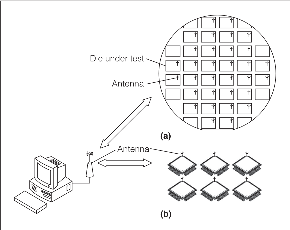 Figure 1: The dual applications of HOY—from wafer-level testing to final chip testing.
2. The Communication Protocol (MAC)
A critical technical challenge was bandwidth. HOY addresses this by using Multicast for test patterns (sending the same data to hundreds of chips at once) and Sequential Polling for responses. This breaks the linear relationship between the number of chips and the time required for data distribution.
Experimental Results: The Economic Shift
The researchers performed a detailed cost breakdown comparing a conventional 180-nm 512-Mbit DDR2 SDRAM test flow against the HOY method.
Key Quantative Findings:
- Total Cost: Conventional (0.31/die).
- Cost Breakdown Change: In conventional testing, ~65% of the cost is wafer test execution. In HOY, the largest cost component shifts to Manufacturing Overhead (58.9%) due to the extra silicon area required for the wireless module.
- Process Scaling: As we move from 350-nm to 65-nm, the absolute area of the HOY test module shrinks, making the "area penalty" for wireless testing virtually negligible (dropping from ~3% to even lower in high-density chips).
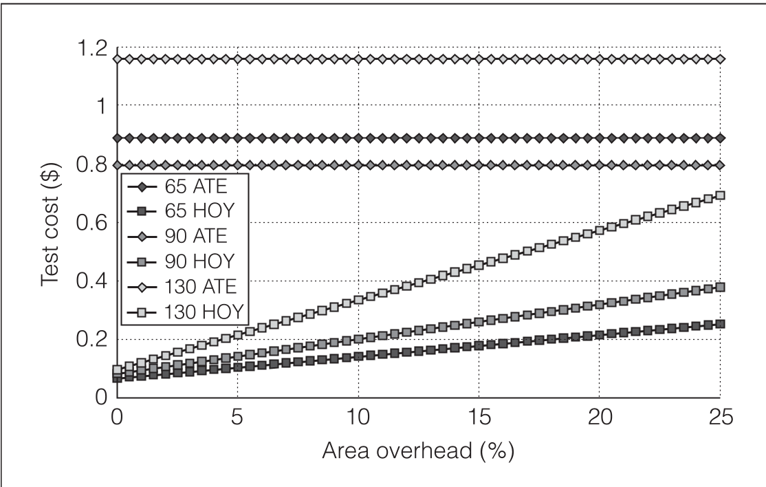 Figure 2: Analysis shows HOY becomes increasingly dominant as die size and test time increase.
Critical Insight: Why Does It Work?
The "magic" of HOY isn't just the wireless radio; it's the redistribution of complexity. Traditional testing tries to make the external machine as smart as the chip. HOY accepts that the chip is already smart and leverages that intelligence (via BIST) to simplify the interface. By removing the hardware-intensive physical contact, we trade a small amount of silicon area for a massive reduction in capital equipment requirements.
Conclusion & Future Outlook
Takeaway: The HOY methodology successfully proves that wireless testing is not only feasible but economically superior for high-volume SoC manufacturing.
Limitations: The "Area Overhead" remains the biggest hurdle for smaller, low-margin analog chips where a 3-5% area increase might outweigh test savings. Future work must focus on further miniaturizing the RF structures and improving the reliability of wireless protocols in electromagnetically noisy factory environments.
As we transition toward 3D ICs and System-in-Package (SiP), where internal layers are physically impossible to probe, wireless methodologies like HOY will shift from being an "alternative" to being the "only choice."