
FPGA-Based BPSK Detection: Bridging the Gap Between Communication Theory and Hardware Realization
13707_An educational digital communications project using FPGAs to implement a BPSK detector.
This paper presents the design and FPGA implementation of an all-digital Binary Phase Shift Keying (BPSK) coherent demodulator using Verilog. It details a student-oriented engineering project involving core DSP components like Booth multipliers and PN generators, successfully prototyped on an Altera 10-k FPGA.
Executive Summary
TL;DR
This paper outlines a comprehensive educational project for implementing an all-digital Binary Phase Shift Keying (BPSK) coherent detector on an FPGA. By leveraging Verilog HDL and Altera 10-k devices, the authors demonstrate how students can build complex signal processing chains—including Booth multipliers, PN generators, and accumulators—to transform theoretical "chalkboard" equations into real-time silicon logic.
Academic Positioning
This work serves as a pedagogical bridge. In the landscape of engineering education, it moves away from pure software simulation (like MATLAB) toward hardware-in-the-loop design. It treats FPGA implementation not just as a tool, but as a discipline that enforces an understanding of timing, resource constraints, and digital fixed-point arithmetic.
Problem & Motivation: The Implementation Gap
In many digital communications courses, students learn that a BPSK receiver requires a correlation process: However, the "Why" and "How" of translating this continuous-time integral into discrete-time digital gates often remain a mystery. Prior educational approaches were often limited by:
- Complexity: Designing at the transistor or gate level was too slow for a single semester.
- Fixed-Functionality: Using off-the-shelf ICs didn't allow students to "see" the internal logic.
- The Abstraction Trap: High-level simulations ignore critical hardware factors like clock cycles, signed multiplication latency, and bit-width growth.
The authors' insight was to use FPGAs as a sandbox, allowing students to design specific sub-blocks (like the 16-bit Booth multiplier) and integrate them into a system that performs maximum-likelihood detection.
Methodology: The Digital Correlation Receiver
The core of the system is a coherent correlation detector. The hardware architecture mimics the mathematical model of a multiplier followed by an integrator.
1. Architectural Components
- ROM-based Carrier Generation: Instead of an analog oscillator, the reference carrier is stored in ROM as sampled data points.
- Booth Multiplier: To handle the signed values of the carrier waves, a serial Booth Multiplier is used. While slower (requiring 32 clock cycles for a 16-bit product), it is resource-efficient and teaches students about the trade-offs between speed and area.
- Digital Accumulator: This block performs the summation (integration). It resets every 8 samples (one bit period) to provide the final statistic for a decision.
2. The Decision Logic
The detector calculates a "statistic" for every bit. If the product of the incoming signal and the local reference is positive, the accumulator grows; if negative (due to a phase shift), it decreases. A simple comparator at the end of the bit interval acts as the decision circuit.
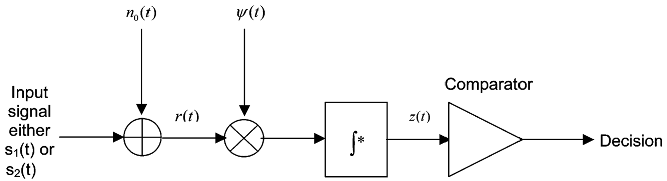 Fig 1: The overall block diagram of the BPSK coherent detection system, illustrating the path from input signal to bit decision.
Experiments & Results
The authors validated the design using Altera Maxplus II and Quartus software. The experiment utilized 8 samples per carrier cycle, with a sampling rate of 1 MHz.
Performance Metrics
- Bit Rate: Approximately 3,720 b/s.
- Clock Frequency: 1 MHz (Scalable upward depending on FPGA speed grade).
- Verification: The simulation showed a perfect recovery of the Pseudo-random Noise (PN) sequence, confirming the logic's correctness.
Key Visualization: Bit Recovery
The simulation results clearly show the phase-locked carrier and the resulting accumulator output. When the input data is "0" (180-degree shift), the accumulator successfully trends negative, leading to a "0" decision.
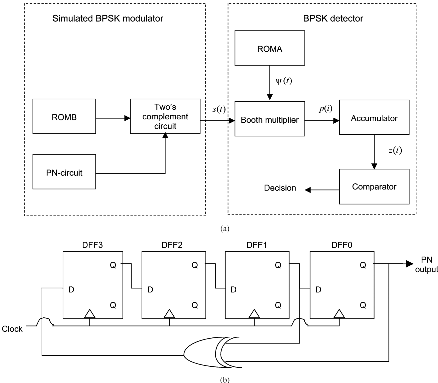 Fig 2: Timing diagrams showing the reference signal, the BPSK modulated carrier, and the resulting accumulator results.
Critical Analysis & Conclusion
Takeaway
The success of this project confirms that HDL-based FPGA design is a viable and necessary component of modern electrical engineering education. It allows for the "physicalization" of complex math without the overhead of custom PCB or ASIC design.
Limitations & Complexity Trade-offs
The use of a serial multiplier is a significant bottleneck. In a high-speed industrial system, a parallel/pipelined multiplier would be required to handle higher carrier frequencies. Furthermore, the paper assumes a perfectly phase-locked reference carrier (generated via ROMB), whereas a real-world system would require a Costas Loop or a Digital PLL to recover the carrier from the noisy received signal—a potential extension for more advanced students.
Future Outlook
As FPGAs continue to incorporate hard DSP slices and SOC (System-on-Chip) capabilities, students can move from simple BPSK to higher-order modulations like QAM or OFDM, using the same fundamental modular design philosophy established in this paper.