
High-Density Memristor-CMOS: Pioneering the First Experimental Ternary Logic Family
2787_High-Density Memristor-CMOS Ternary Logic Family.
This paper presents the first experimental demonstration of a complete ternary memristor-CMOS logic family. Utilizing in-house fabricated Indium-Tin-Oxide (ITO) memristors with built-in selectors, the authors successfully implement primitive and combinational ternary gates (AND, OR, NOT, NAND, XOR, etc.), achieving a significant milestone in multi-valued logic hardware.
TL;DR
Researchers have successfully moved ternary logic from theoretical simulation to physical hardware. By integrating in-house fabricated ITO (Indium-Tin-Oxide) memristors with a 50-nm CMOS process, they created a logic family that computes with three states (0, 1, 2) instead of the binary (0, 1). This breakthrough delivers up to 25x higher data density and 13x faster switching speeds compared to previous ternary memristive benchmarks.
The "Radix Dilemma" in Modern VLSI
Since the 1960s, engineers have known that ternary (Base-3) logic is theoretically more efficient than binary for data density. However, implementing it in pure CMOS often requires double or triple the transistor count to handle the intermediate voltage levels, leading to an "area penalty" that eats up all theoretical gains.
The researchers identified three primary killers of ternary logic:
- Area Consumption: More gates needed for the same function.
- Propagation Delay: Cascaded stages slow down significantly.
- Noise Tolerance: The reduced gap between voltage levels makes the system fragile.
Methodology: Vertical Integration and Built-in Selectors
To solve the area and noise issues, the team leveraged Memristor-CMOS integration. Instead of spreading logic "outwards" on the silicon surface, they built it "upwards" using the Back-End-of-the-Line (BEOL).
1. The ITO Memristor Architecture
The heart of this work is a V/ITO(O2)/TiN structure. Unlike standard RRAM, this device features a self-oxidized Vanadium layer that acts as a built-in "selector." This is critical because it acts like a microscopic switch that prevents "sneak path" currents—a notorious problem that ruins noise margins in multi-level logic.
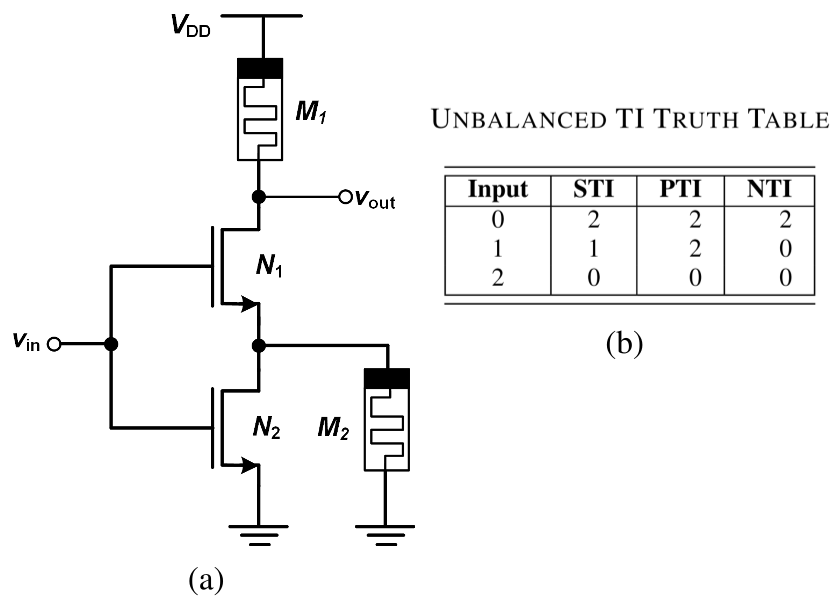 Fig 1: The proposed Ternary Inverter (STI) schematic and the foundational Truth Table for the logic family.
2. Logic Implementation: TAND, TOR, and TI
The logic family uses unbalanced positive ternary logic where heights correspond to (GND, VDD/2, VDD).
- TAND & TOR: These function as the MIN and MAX operators of the two inputs.
- Ternary Inverter (TI): Uses NMOS sizing and memristive pull-ups to define the threshold for switching between the three logic states.
Experimental Results & Performance Benchmarks
The team validated the design through both SPICE simulations and board-level hardware prototyping of encoders and decoders.
Speed and Density
The switching speed reached ~30 ns. While still slower than the sub-nanosecond transit times of pure CMOS transistors (due to the ionic nature of memristors), it represents a 13x leap over previous ternary memristor efforts.
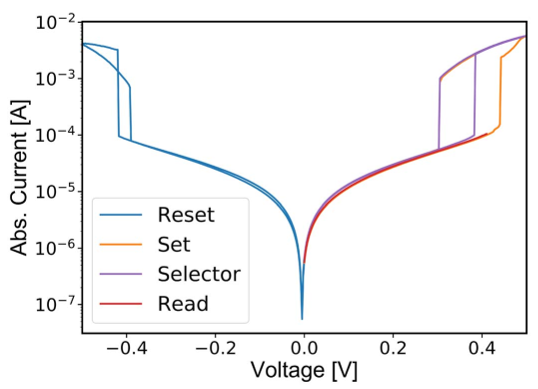 Fig 2: I-V characteristics of the fabricated ITO device showing the selector-dominated low-leakage region (red) and rapid switching.
Comparative Analysis
| Metric | This Work (Ternary) | Conventional CMOS (Binary) | Improvement |
|---|---|---|---|
| Data Density | High (Base-3) | Standard (Base-2) | 3.9x - 25.5x |
| Switching Speed | 30 ns | ~10 ps | CMOS remains 1000x faster |
| Power Efficiency | ~30-65 μW | ~nW | CMOS is more efficient |
Critical Insight: Why This Matters
The most profound takeaway is the Area-Density Validation. Most academic papers claim ternary logic is "better" based on transistor count. This paper proves that sizing is everything. For instance, as shown in Table VI, a Simple Ternary Inverter (STI) is actually smaller than a Negative Ternary Inverter (NTI) because the STI requires less aggressive transistor sizing to function, despite having more components.
Limitations & Future Outlook
While the density gains are astronomical, the static power dissipation remains much higher than CMOS. This is because memristor-based logic is fundamentally "ratioed" logic (like ancient NMOS logic), meaning current flows whenever the gate is active.
Future research must focus on:
- Power Reduction: Transitioning from ratioed logic to something resembling "push-pull" complementary memristive logic.
- Endurance: Moving beyond the cycle limit to reach the + cycles required for general-purpose logic.
Conclusion: This work is a massive step toward "Computing-in-Memory" and high-density storage controllers. It proves ternary logic is no longer just a mathematical curiosity but a manufacturable reality.