
Magnetic Adder: Bridging the Gap Between Logic and Racetrack Memory
Magnetic Adder Based on Racetrack Memory
This paper presents the first design of a fully non-volatile multi-bit Magnetic Adder (MA) utilizing Perpendicular Magnetic Anisotropy (PMA) Domain Wall (DW) racetrack memory. By integrating Magnetic Tunnel Junctions (MTJ) directly with Pre-Charge Sense Amplifiers (PCSA), the authors achieve a "logic-in-memory" architecture that eliminates the separation between computing and storage.
TL;DR
Researchers have developed a fully non-volatile multi-bit adder that stores data in magnetic "racetracks" instead of volatile CMOS latches. By performing "logic-in-memory," this design eliminates standby power leakage and significantly reduces the silicon area required for complex arithmetic operations, achieving a 4.5x area reduction for an 8-bit serial adder.
Context: The End of the CMOS Era?
As CMOS scaling hits the physical limits of leakage current and heat dissipation, the industry is searching for materials that offer non-volatility and infinite endurance. Spintronic devices, specifically Magnetic Tunnel Junctions (MTJ), have emerged as the frontrunners. However, early magnetic adders were often "hybrid" or "partially non-volatile," still relying on CMOS to move data around. This paper takes a leap forward by using Racetrack Memory (RM) to create a serial adder where even the intermediate carries and shift registers are entirely magnetic.
Problem & Motivation: The Data Movement Bottleneck
In standard Von Neumann architectures, data constantly shuttles between the CPU and Memory. This creates:
- Standby Power Leakage: Volatile registers need constant power to "remember" bits.
- Interconnect Delay: Moving bits across the chip takes time and energy.
- Area Overhead: Implementing a non-volatile flip-flop (NVFF) using traditional MTJs often requires large current sources that eat up die area.
The authors' insight was to use Domain Wall (DW) motion. Instead of switching a single MTJ for every bit, why not "shift" magnetic domains along a nano-wire?
Methodology: Logic-in-Memory via Racetracks
The core of the system is the Pre-Charge Sense Amplifier (PCSA). This circuit compares the resistance of two magnetic networks. If the left branch's resistance is lower than the right, it outputs a logic "0," and vice versa.
1. The 1-Bit MFA Core
The adder utilizes a Majority Function for the Carry () and a XOR-based network for the Sum. By arranging MTJs in series and parallel configurations, the PCSA evaluates the boolean logic directly from the magnetic state of the racetrack.
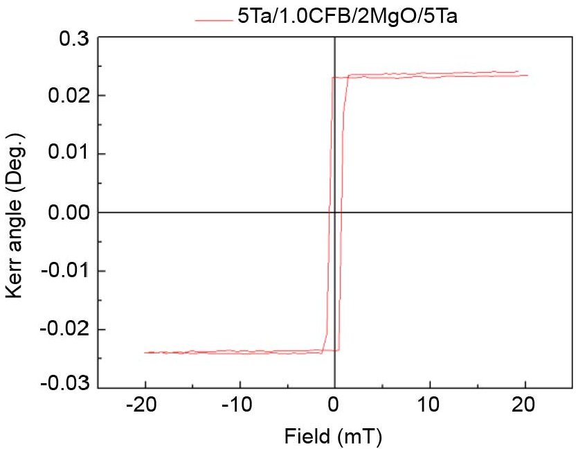 Fig. 1: Racetrack memory concept showing DW nucleation (Writing) and TMR detection (Reading).
2. Multi-bit Serial Architecture
For an 8-bit addition, the data resides in two magnetic stripes ( and ). On each clock cycle:
- The LSB (Least Significant Bit) is sensed.
- The Sum bit is written into a new "Sum" racetrack.
- A shift current () moves the next bit into position under the read head.
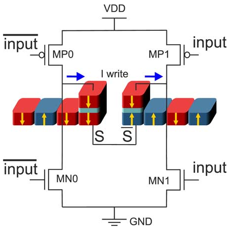 Fig. 2: Schematic of the proposed Magnetic Full Adder (MFA) integrated with the PCSA.
Experiments & Performance Аналитика
The team used a 65nm CMOS process combined with a Verilog-A model of CoFeB/MgO PMA racetracks.
- Area Efficiency: The magnetic adder occupies only 34 compared to the 155 required by a standard CMOS serial adder—a 4.5x reduction.
- Standby Power: 0 Watts. Because the state is held in the magnetization of the racetrack, you can pull the plug and resume calculation instantly upon power-up ("Instant ON/OFF").
- Dynamic Energy Optimization: The authors noticed that writing (nucleating) a new magnetic domain is expensive. They introduced an Optimization Design using a comparator. If the new Carry bit is the same as the old one, the writing circuit stays OFF, saving 50% of switching energy on average.
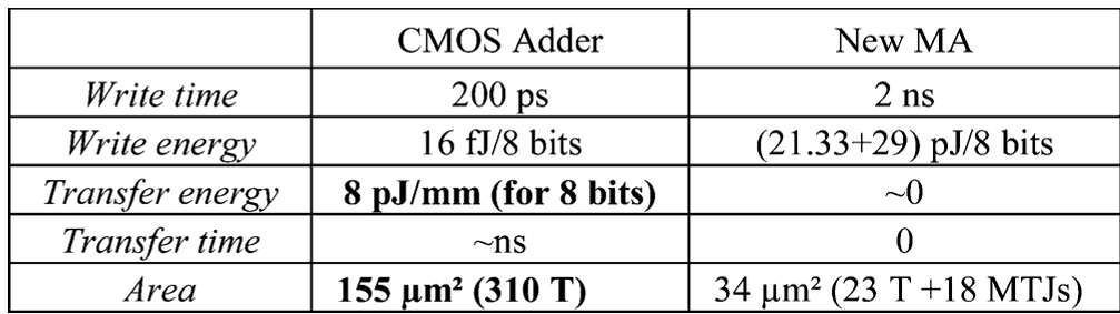 Table 1: Comparison between CMOS Adder and the proposed Magnetic Adder (MA).
Critical Insight: The Energy-Delay Tradeoff
While the area and standby power gains are massive, the "tax" is dynamic energy. Nucleating a domain wall requires high current density. The paper shows that while logic sensing is incredibly fast (~180 ps), the total cycle is bottlenecked by the DW motion and nucleation time (~2 ns). This suggests that while this technology is perfect for high-density, low-power "normally-off" sensors or IoT devices, it might need further material optimization (like SOT - Spin-Orbit Torque) to compete with high-performance CPU caches.
Conclusion
This paper provides a blueprint for a Magnetic CPU. By successfully demonstrating an 8-bit serial adder where the memory is the logic, the authors have proven that we can move past the constraints of volatile CMOS registers.
Key Limitation: The current required for DW motion remains high, leading to dynamic energy consumption 6x higher than CMOS for active switching. Future research into low-current SOT-driven motion will be the key to unlocking this technology's full potential.