
Global Nanoelectronics: Mapping the "Beyond CMOS" Frontier and Its Hidden Gaps
Regional, National, and International Nanoelectronics Research Programs: Topical Concentration and Gaps This survey of electric research programs aims to encourage international collaboration; examples of collaborative programs are provided and funding sources are identified.
This paper presents a comprehensive survey by the International Planning Working Group on Nanoelectronics (IPWGN) regarding publicly funded research programs in Europe, Japan, and the United States. It maps global R&D efforts against the International Technology Roadmap for Semiconductors (ITRS) to identify strategic "Beyond CMOS" research concentrations and critical gaps.
TL;DR
The microelectronics industry is hitting a wall. As traditional CMOS scaling reaches its sunset, an international working group (IPWGN) has audited the world's research output. They found that while we are obsessed with building better "switches" and "architectures," we are dangerously ignoring the physical "housekeeping" of computing—specifically thermal management and non-equilibrium physics.
The Scaling Paradox: Why Motivation Matters
For decades, the "Moore's Law" engine was simple: shrink the transistor, and everything gets better. Today, scaling brings diminishing returns and escalating heat. The authors argue that the "Beyond CMOS" era is currently too pre-competitive and high-risk for any single nation to solve. The motivation for this paper is to act as a global "GPS," showing where the research funding is flowing and, more importantly, where it is missing.
Methodology: The Seven Vectors of Computing
To make sense of thousands of disparate projects, the IPWGN adopted the Research Vectors defined by the ITRS and the Nanoelectronics Research Initiative (NRI). These vectors move beyond "charge" as the only way to process information, looking instead at spin, phase, and even biological paradigms.
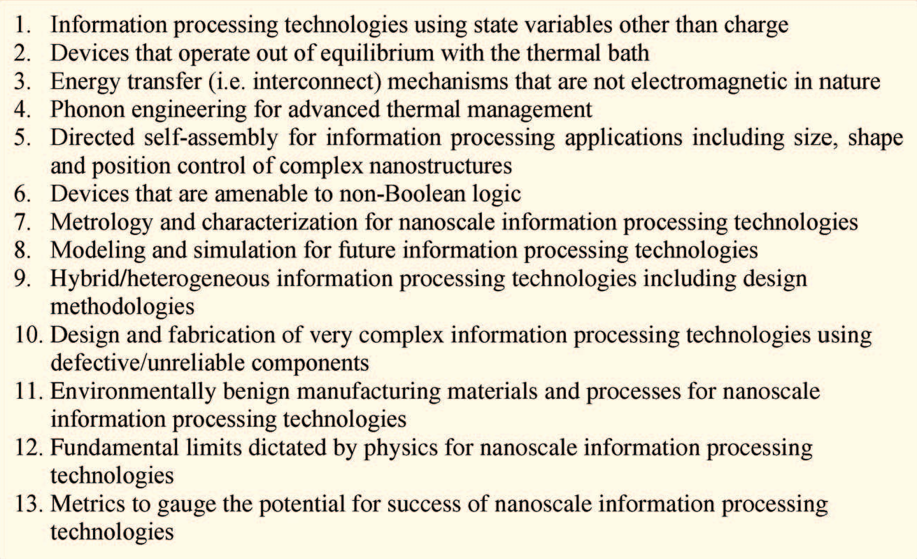 Table 1: The 13 critical research vectors required to sustain information technology progress.
The researchers divided the world into two camps:
- Computation and Storage: The core logic and memory.
- More-than-Moore: Sensorial and power-management functionalities that don't follow traditional scaling.
Regional Deep-Dive: A Tale of Three Geographies
Europe: The Architectural Focus
European funding (via FET and EC programs) shows a balanced interest in nanodevices, but with a unique strength in Emerging Architectures. However, like its peers, it lacks depth in thermal management.
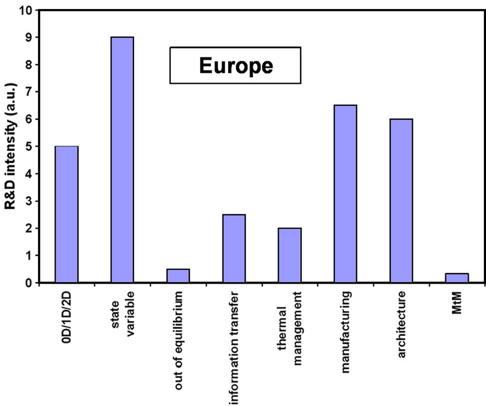 Fig 1: European project distribution highlights a "More-than-Moore" gap.
Japan: The Device Powerhouse
Japan’s programs (METI/NEDO) are heavily weighted toward Nanodevices and Fabrication Techniques. They have a notable investment in 3D integration (the "Dream Chip" project), yet they share the global "blind spot" for out-of-equilibrium computation.
USA: The Interconnect & Switch Quest
In the US, the Nanoelectronics Research Initiative (NRI) and NSF focus heavily on finding the "New Logic Switch." While the US leads in "Information Transfer" (interconnects), it falls behind in disruptive manufacturing and thermal engineering.
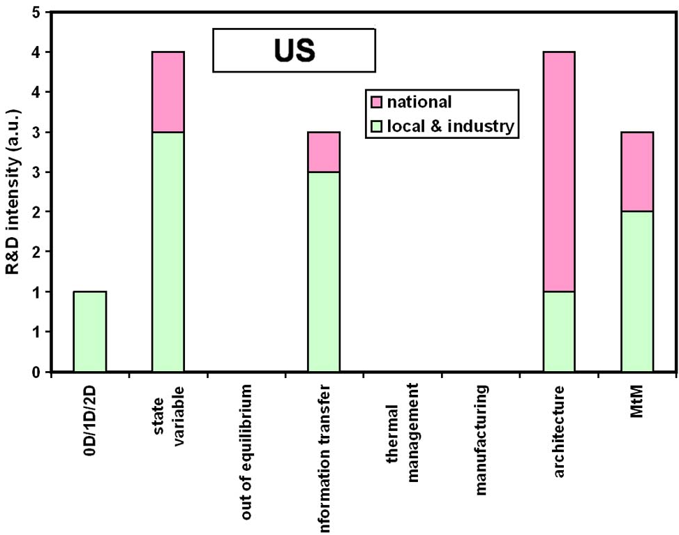 Fig 3: US spending highlights priorities in devices and architectures.
The Verdict: Where are the Gaps?
The most striking takeaway from this paper is the universal neglect of thermal management and phonon engineering. While we strive for smaller, faster chips, the fundamental physics of how heat moves at the nanoscale remains under-funded.
The authors also highlight Out-of-Equilibrium Computing—systems that don't rely on thermal bath stability—as a nearly vacant field. This is a critical risk; without solving heat and noise, even the most perfect "Beyond CMOS" switch will fail in a practical system.
Conclusion and The Path to Collaboration
The IPWGN doesn't just point out problems; it provides a roadmap for Interregional Collaboration. By identifying specific funding tools (like the NSF/OISE PIRE program or the European FP7 framework), the authors encourage researchers to bridge these gaps through trans-border partnerships.
Final Insight: The future of nanoelectronics isn't just about the next transistor—it's about the thermal and architectural ecosystem that allows that transistor to function. If the industry doesn't address the "cold" side of computing, the "Beyond CMOS" era will be very short-lived.