
Intel Xeon® E5-2600 v3: Redefining Server Efficiency with FIVR and 18-Core Haswell Architecture
The Xeon® Processor E5-2600 v3: a 22 nm 18-Core Product Family
The Xeon® Processor E5-2600 v3 (Haswell-EP) is a 22nm enterprise-grade server CPU featuring up to 18 cores and 45MB L3 cache. It leverages Intel's Tri-gate technology and introduces Fully Integrated Voltage Regulators (FIVR) alongside DDR4 support to achieve a 33% performance boost over its predecessor.
TL;DR
The Intel Xeon® E5-2600 v3 (codenamed Haswell-EP) represents a landmark shift in enterprise silicon. By integrating 18 dual-threaded cores, adopting the first-ever DDR4 support, and most importantly, moving power regulation onto the die via Fully Integrated Voltage Regulators (FIVR), Intel achieved a 33% performance leap. This work is not just a core-count bump; it is an architectural masterclass in power delivery and modularity.
The Power Delivery Crisis
Before the E5 v3, server motherboards were becoming nightmarishly complex. Delivering high current at low voltages (~1V) caused massive resistive losses in the motherboard traces. Moreover, in previous "Per-Socket P-State" models, if one core demanded a high-frequency "Turbo" boost, every core in the socket was forced to ramp up voltage, wasting immense amounts of power. This lack of granularity was the primary bottleneck for power-constrained data centers.
Methodology: The FIVR Revolution
Intel’s solution was to bring the regulators onto the silicon. The FIVR system receives a relatively high 1.8V from the motherboard (reducing current and resistive loss by a square-law factor) and converts it to the exact required voltage on-die.
1. Per-Core Granularity
With 31 independent FIVR supplies on a single 18-core die, the PCU (Power Control Unit) can assign each core its own voltage-frequency point. This enables Per-Core P-States (PCPS)—only the cores doing the work consume the power.
2. Physical Implementation (ACIs)
To make this work without massive external components, Intel used Air Core Inductors (ACI) built directly into the package layers.
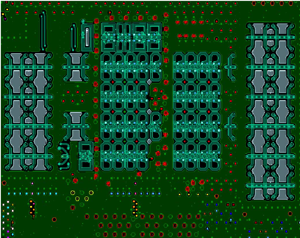
3. Modular "Chops"
The design is modular. Intel created three "chops" (18-core, 12-core, and 8-core) to address different market segments while reusing the same fundamental IP. By aligning clock and power domains to these chop lines, they minimized redesign efforts for different SKUs.
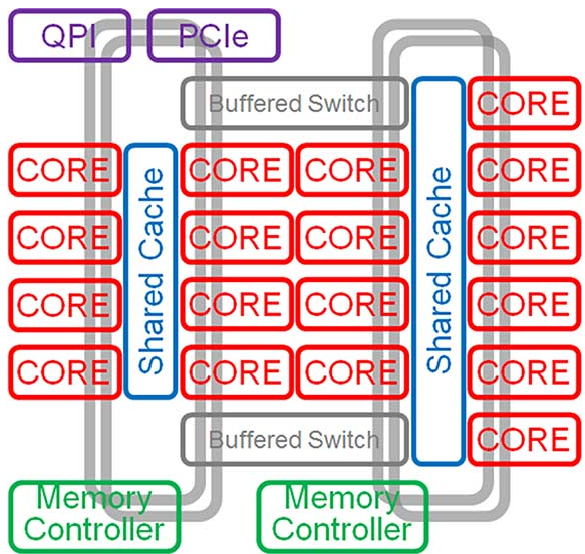
Experiments & Results: Efficiency at Scale
The impact of FIVR and the Haswell microarchitecture is evident in the power-to-performance metrics:
- Power Savings: On a 145W TDP SKU, the efficiency gains from integrated regulation and 8 unique voltage curves per core resulted in a 20W saving.
- Memory Prowess: The new DDR4 interface supports up to 2133 MT/s. Despite the higher speed, it consumes 38% less power and 40% less area than the previous DDR3-only design.
- Heterogeneous Workloads: As shown in the benchmarking, PCPS allows for significantly lower power consumption when utilization is below 100%, as inactive cores aren't dragged to high voltage states.
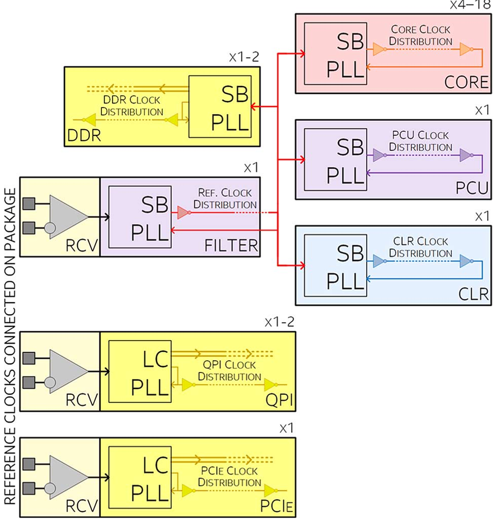
Critical Analysis & Conclusion
The E5-2600 v3 was a pivotal moment for Intel. It proved that on-die regulation is the only way to sustain core-count scaling.
Takeaway: The move to FIVR wasn't just about saving power; it was about control. By decoupling the voltage of the "Uncore" (cache/ring) from the "Core," Intel allowed the ring interconnect to remain at high frequency for low latency while cores remained in low-power states.
Limitations: While FIVR provides incredible granularity, it inherently increases die size (roughly 1% for the bridges alone) and introduces thermal hotspots. In later generations, Intel briefly moved away from FIVR due to these thermal complexities before returning to similar integrated strategies.
Future Outlook: The techniques pioneered here—Modular design through "chops" and granular power domains—laid the groundwork for the modern chiplet-based era where power management is the's heart of the system architecture.